Quarantine has been a rare chance to spend some quality time at the bench.
AF1R of the Wellesley Amateur Radio Society started a 10 meter local net on Thursday nights on 28.3333333333 MHz. My existing rigs are built for 40m and 2m so I've been stuck listening. That gave me the perfect excuse to go build something! The result was a 10m side-band transmitter that runs about 12 watts. Total construction time was 3 weeks. Signal reports from the net have been good. I use this transmitter with my direct conversion receiver that has been modified for use on 10m. There is so little activity on 10 meters that I don't need to worry about anyone on the "other side" of zero-beat in the DC receiver passband. All good.
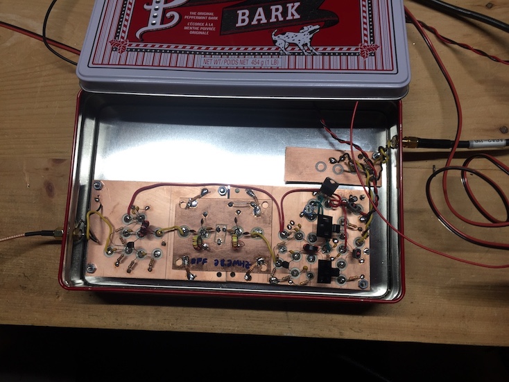
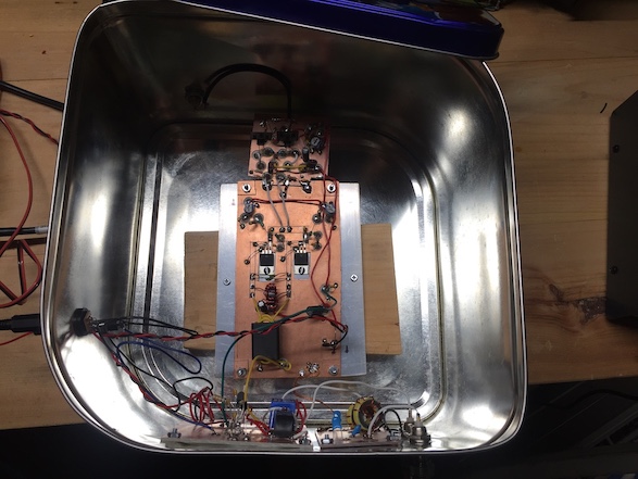
The finished rig is shown below. I've been saving these nice candy/cookie tins since Christmas. There is nothing that warms the heart of a homebrewer more than a holiday gift in a beautiful square or rectangular tin. Even an empty rectangular tin with a nice ribbon is a treasured gift! But those round tins? Well ... it's the thought that counts.
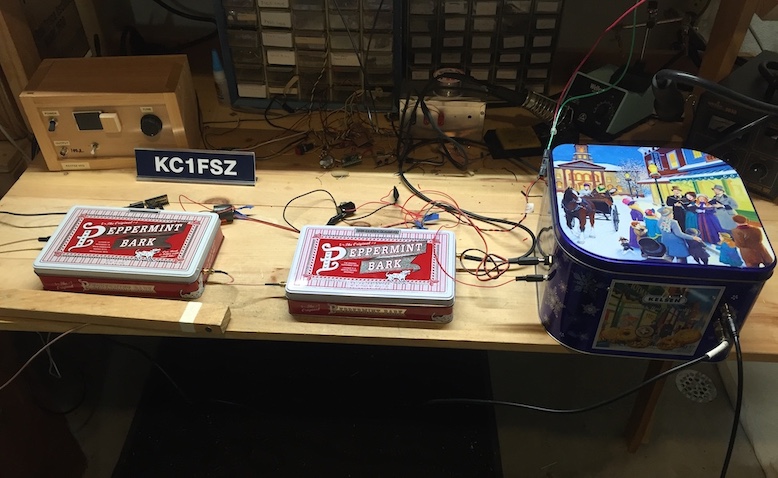
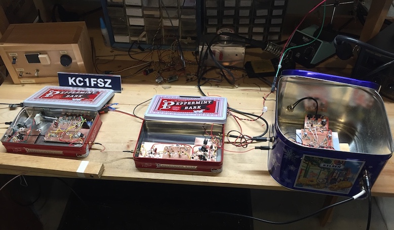
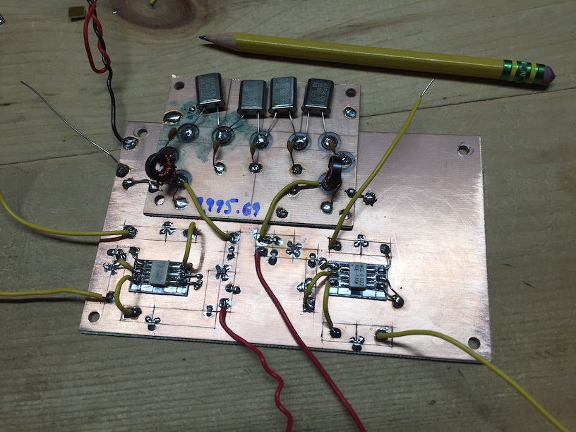
Covers off. This is a modular design because I am planning to re-use the parts. Plus modular construction makes quality assurance much easier. The first module (left) is the mic amp, balanced modulator, crystal filter, and RF mixer. The second module (center) is more amplification and the band-pass filter. The third module (right) is the driver, PA final, LPF, and T/R relay. Short SMA cables connect the modules.
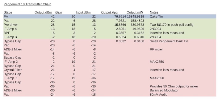
There's no schematic because I was following the JMTSU™ design methodology. But I've found that creating a spreadsheet that accounts for the gains/losses of the different stages helps even more than a schematic. Plus I'm a financial services IT guy so I like having a profit and loss sheet for everything. Here's my sheet for this rig. The different colors are the different modules. Output on top, input on the bottom.
I'll walk through the parts in more detail.
Here's a close-up of the SSB exciter module:
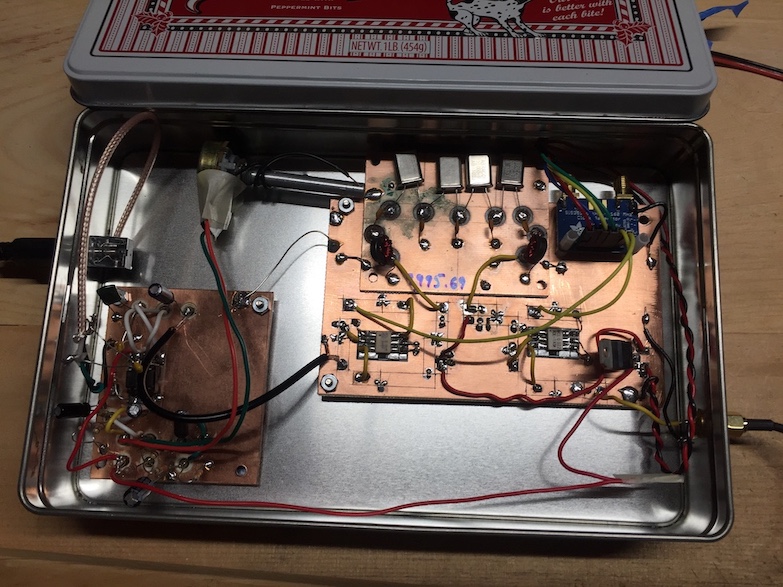
The microphone is an electret capsule mounted into a 1x2 piece of wood. The microphone cable is RG-178 coax for good shielding. The next stage is a TL072 dual low-noise op-amp. The first op amp is the microphone gain stage and the second is an audio band-pass filter. Next is the SSB modulator. This is a single-converstion architecture with a ~10 MHz IF, upper side-band. The balanced modulator is a Mini-Circuits ADE-1 mixer with 6dB pads on all ports. The SSB filter uses 4 crystals sorted from a bag of 20 or so. The completed filter measured out at 9995 kc with a 3 kc passband. I've been told it sounds a bit too narrow. Transformers are used to get impedances up/down to/from 200 ohms. The RF mixer is another ADE-1 mixer which gets us up to 28 MHz. Again, 6dB pads on all ports of the mixer. The buffer amplifiers are very small +19dB monolithic RF gain blocks made by Maxim (MAX2650). $2.00 each. I really like these things. They are good up to -1dBm so are perfect for the IF stages. The mixers are driven by two channels of an SI5351/A controlled via an I2C bus. The controller is a Teensy 3.2. All very standard stuff on the digital side so I won't bother with that detail.
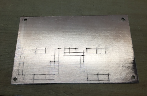
I decided to try something different on this part of the build and I used surface-mount parts. I like how this goes together and the next iteration of this build could be much more compact. The SMD components are mounted on a normal copper-clad PCB which has been hand-milled using an X-Acto knife and a metal ruler. For other projects I've had PCBs made using the commercial fabricators (OshPark/JLC/etc.). It's cheap, but I hate waiting 10 days for the boards to arrive. By the time the boards show up I've usually found a bug or changed the design! With a bit of planning/sketching/patience you can create a nice layout by hand. The ADE-1s are also surface-mount but I keep these on small daughter-cards (W1REX Me-Pads) so I can re-use them easily in other circuits. These mixers are the most expensive components in the rig at around $8 a piece.
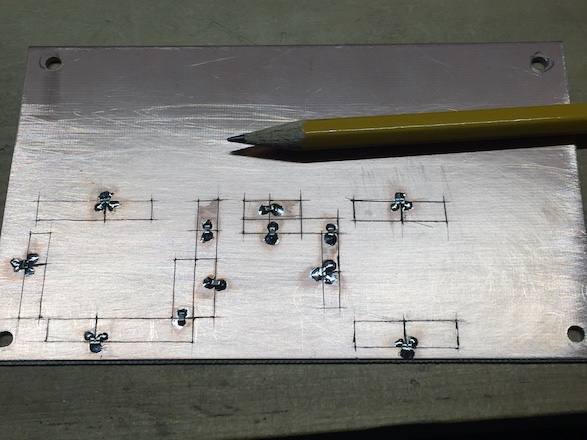
Here's the board all hacked up and ready for assembly:
All attenuator pads and bypass/decoupling capacitors installed. I'm using 0805 SMD parts. Pretty small, but it works great!
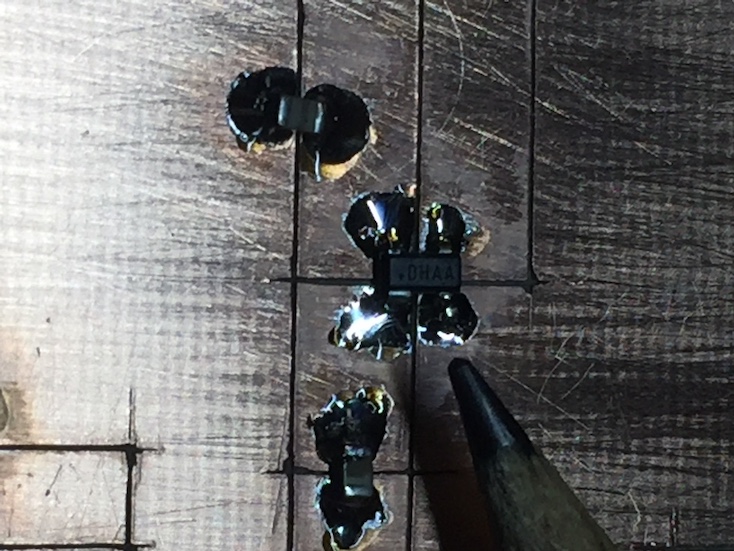
Here's one of the MAX2650 RF gain blocks. You can use your iPhone for close-up inspection of SMD solder joints.
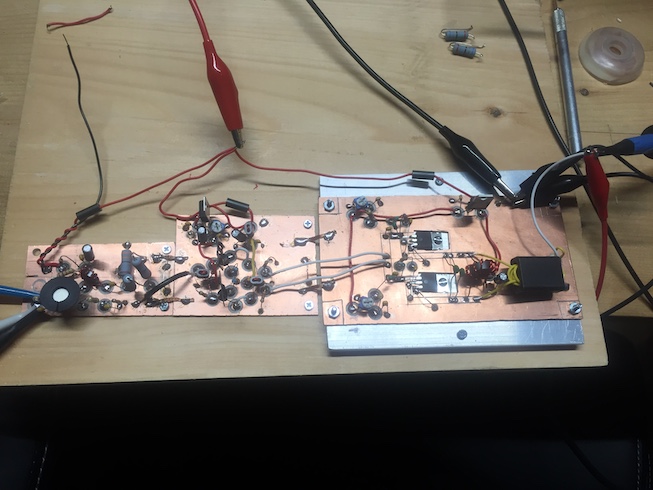
Up and running on the test bench:
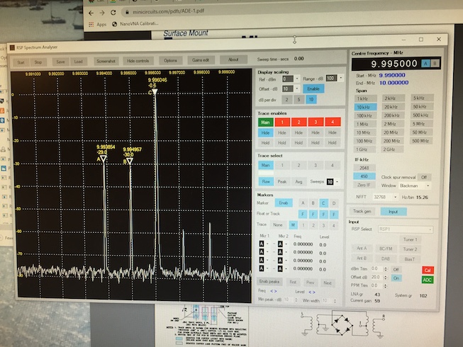
One tool that I've really come to appreciate is the combination of my SDRPlay receiver and the Spectrum Analzer software written by Steve Andrew. For $100 you've got yourself a full-featured spectrum anlyzer. I use this more than my oscilliscope now. Here's a look at the first conversion and SSB filter stages. Opposite side-band/carrier supression shows about -30dB. Not great, but good enough for now.
This module starts with a 2N3904 feedback amplifier. Then a band-pass filter to eliminate the mixing image. Next is another 2N3904 feedback amplifier. Next a pre-driver stage made using two BS170 MOSFETs in push-pull configuration. Lastly, a 6dB pad for stability. This module is pretty basic.
One thing I really enjoyed about this project was getting to know my NanoVNA better. I've had this $55 device for a few months but I never had the time to really get into its details. I highly recommend this amazing tool because it takes a lot of the guesswork out of filter building. It feels like cheating.
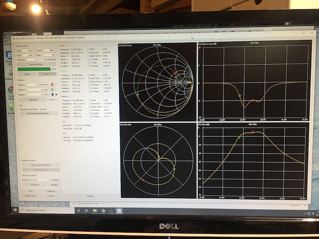
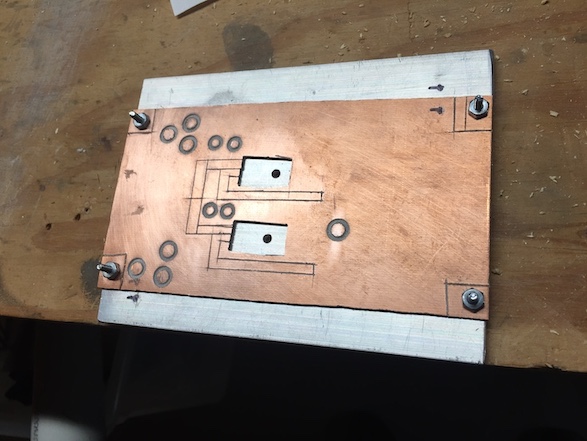
I used the equations in EMRFD for the doubly-tuned LC band-pass filter. Here's a view after tweaking the coil counts a few times. Got to like that.
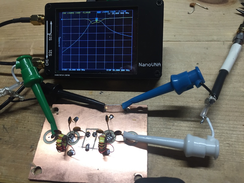
Here is the companion software on the PC called NanoVNASaver. Hats off to 5Q5R for writing this great program.
This is the hardest part. RF power amplifiers are never easy. My design is another dual-BS170 push-pull driver stage into a push-pull IRF510 pair. Very standard stuff. Biasing of both stages is manual using some trim pots. Bias is 100mA for each IRF510 and another 25mA for the BS170s.
Here's a look at the power board and heatsinks. I'm just using an aluminum bar that I happened to have. The IRF510 drains are bolted diectly to the heatsinks so the two heatsinks need to be electrically isolated from each other and from the rest of the rig. Notice the cuts in the PCB around the corner screws. Everything is bolted to a wooden block to insulate it from the chassis. After a long QSO you have a nice aroma of smoldering wood which further enhances the winter holiday theme of the rig. Chesnuts roasting on an open MOSFET. I'm adding a fan to the PA tin but I'm worried that it might just fan the flames. Next time I'm going to do the thermal coupling thing and keep the FETs electrically isolated from everything else - much less hassle I think.
Here's the finished amplifier being tested. I needed a fair amount of degenerative feedback to keep it stable. That costs me a few dB. And good metal enclosures are critical for stabilty at this power level. But the finished product is reasonably linear and very reliable.
I'm good on QRZ. Send me an e-mail if you have any questions. No, there is no schematic. 73s! Bruce KC1FSZ.